Welcome: Shenzhen Zhuolida Electronics Co.TD
Language:
 ∷

∷
∷
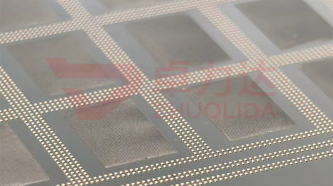
A 12-inch wafer bumping stencil has passed ±3 μm aperture checks and ±7 μm total pitch, yet the whole field fails to register on the bonder. The problem is rarely the apertures; it is the handful of datum holes. Wafer bumping stencil datum hole forming governs how those reference holes grow together with the apertures: the datum holes are the only reference the tool uses to recognize the plate and align the wafer, so a small shift moves the coordinate frame of tens of thousands of apertures. Error accumulates stretch by stretch — master datum, LDI double-side alignment, electroforming distortion, framing stress — each contributing a little, and the sum has to stay inside ±7 μm. The line does not drill datum holes afterwards, since drilling adds a fresh clamping error; apertures and datum holes share one exposure and one electroforming run so they sit in the same coordinate frame. Roundness has to reach ±0.002 mm, measured on its own with a vision system, before the datum chain is closed.
The common trap is treating datum holes as small holes to be drilled later. A batch runs true for the first few wafers, then the whole field drifts to one side; apertures still measure inside ±7 μm, but framing stress has pulled a datum hole oval, so the locating pin drags the plate off as soon as it seats. Switch exposure lots and the front and back datum holes differ in alignment by around 5 μm, consuming the ±5 μm double-side budget with no room left to register. Subtler still is local distortion: on a 610×660 mm plate edge stress is uneven, one edge datum shifts more than the centre, the checker scanning openings misses it, and the four corners only fail to match at assembly. None of these show in a single ±3 μm aperture re-check, which is why wafer bumping stencil datum hole forming pulls the whole datum chain out to measure rather than passing one hole.
Parameter Window
• Position: cumulative datum error ±7 μm, aperture accuracy ±3 μm, datum holes drawn on the same artwork
• Roundness: datum hole ±0.002 mm, vision system measures roundness separately, not folded into the aperture item
• Double-side alignment ±5 μm, front and back datums transferred in one exposure, no secondary drilling
• Maximum substrate 610×660 mm, alignment drift sampled at edge, centre and corner
• Tension 10–55 N (±1 N internal); uneven framing stress drags datum holes off
• LDI resolution 8 μm/8 μm, master datum marks and apertures in one coordinate frame
Manufacturing Process (8 Steps)
1. Artwork preparation — apertures and datum holes on one master, datum marks in a single coordinate frame.
2. Pre-treatment — substrate cleaning and conductive coating, mandrel passivated against strike nodules.
3. Lamination and LDI — ±5 μm double-side alignment, datum holes and apertures formed in one exposure.
4. Development — control concentration and time so datum walls stay vertical and rims neither collapse nor shrink.
5. Electroforming — staged nickel-cobalt at 1–4 A/dm² with low-temperature annealing to stop datum drift from stress.
6. Demolding — one-piece release from a low-stress corner, the datum zone never lifted first.
7. Inspection — vision system for ±7 μm position and ±0.002 mm roundness, flash measurement re-checks apertures.
8. Framing and packing — AB adhesive frame, tension within a 10–55 N band, assembly datum logged per lot.
Core Advantages
1. Stable registration — hold wafer bumping stencil datum hole forming at ±7 μm and the whole aperture frame stays put.
2. No error stacking — one shared exposure removes the clamping error of secondary drilling.
3. Roundness controlled — ±0.002 mm measured separately, so locating pins do not bind.
4. Accurate on large plates — three-point sampling on 610×660 mm keeps edge drift in view.
5. Stress kept out — annealing and tension bands stop framing from dragging the datum.
6. Traceable — master coordinates, alignment data and assembly datum filed per lot for fault tracing.
Typical Applications
1. WLP wafer bumping templates for 4–12 inch wafers, apertures registered to the wafer through datum holes.
2. Ball and Flux stencils for ABF substrates, where stacked printing demands matched datums.
3. Positioning plates in semiconductor exposure and alignment carriers, where pin fit is tight.
4. Precision screens and grading meshes, where frame datum sets whole-sheet alignment.
5. Composite stencils with post height or local thickening, whose step zones drift more readily.
6. Large-format photovoltaic grid stencils, where edge datum drift matters most.
Design and Selection Notes
1. Fix the datum scheme first. Draw apertures and datum holes on one artwork, leave no downstream drilling.
2. Keep a single master coordinate frame, front and back datum marks aligned in one pass.
3. Do not rush development; a collapsed rim lets the locating pin drag the whole plate off.
4. Sample edge, centre and corner on large plates, not only the hole at the centre.
5. Anneal before framing; leave the stress in and ±7 μm cumulative error will not hold.
6. Give datum recheck its own station — a checker reads neither roundness nor coordinate drift.
7. Set tension within one of the 10–55 N bands with ±1 N internal control, never mix bands in a lot.
Seen on its own, wafer bumping stencil datum hole forming occupies no standalone step: the datum mark is fixed in the master, front and back are aligned in one LDI pass, electroforming and annealing decide whether stress moves that coordinate, and framing adds one more force to it. Master, exposure, deposition, stripping and framing each own a stretch, and let any one slip and ±7 μm cumulative error piles up, the whole aperture field shifting with it. What is hard on a line is not one plate with a perfect datum now and then, but a dozen plates from one bath and several consecutive lots sitting in the same hole position, roundness and assembly datum band — only then does ±3 μm aperture accuracy mean anything. For orders with a hard requirement on registration, fix the master coordinate frame, double-side alignment data, anneal curve and tension band into the process card at sampling stage; it is cheaper than shimming the plate into alignment after assembly. On paper wafer bumping stencil datum hole forming is a string of tolerances; on the line it is every plate seating in the same position the moment the pin goes in.
Contact:赖先生
Phone:+86 18938693450
Tel:0755-2708-8292
Email:yw9@zldsmt.com
Add:深圳市宝安区福永镇新和村福园一路华发工业园A3栋
 Zhuolida
