Welcome: Shenzhen Zhuolida Electronics Co.TD
Language:
 ∷

∷
∷
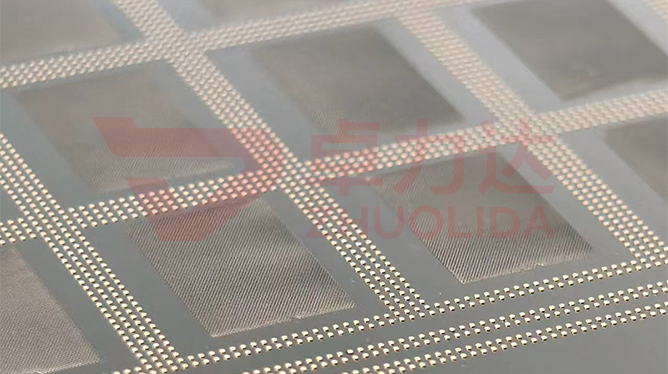
A bumping stencil with 30 μm apertures passes ±3 μm aperture and ±7 μm position checks, yet after a few thousand prints it starts skipping balls and laying down uneven volumes. Strip it down and the openings are unchanged; a tacky film of flux clings to the walls. Bumping stencil flux residue control governs where that film comes from, how it is cleaned and how it is verified: the residue itself arrives from the printer, but whether it sticks is decided by the stencil wall. A smooth wall free of resist residue and nodules gives flux little to grip and lets one wipe clear it; a wall with pits or development residue traps flux in the hollows, and wiping only pushes it deeper. The line holds wall roughness to Ra ≤ 0.01 μm, cleans in separate baths after demolding, and judges cleanliness by ionic contamination plus microscopic sampling. The goal is not a bright plate before printing, but a wiping interval that still follows its curve as print life approaches 15,000 cycles.
The common trap is blaming the whole problem on the flux type at the printer. One batch clogs at the 30 μm rims after three thousand prints while other lots run to end of life; wiping will not clear it, and sectioning shows fine nodules holding flux in the pits. Switch development baths and undeveloped resist mixes with flux into a film — aperture size is unchanged but throughput drops first. Worse is over-cleaning: a long solvent soak dulls the nickel and roughens wall Ra, so the plate clings to flux more than before, and the customer only finds out after returning the lot. None of these show in a routine ±3 μm aperture re-check, which is why bumping stencil flux residue control pulls cleanliness out for its own check, tracking ionic contamination and microscopic sampling lot by lot rather than waiting for skipped balls at the bonder.
Parameter Window
• Wall roughness: Ra ≤ 0.01 μm ceiling, a smooth wall gives flux little to cling to
• Print life: 15,000 cycles target, wiping interval set by the residue accumulation curve
• Minimum aperture 30 μm, where residue bridges rims most easily and sampling starts
• Cleaning: aqueous and solvent baths separated, temperature and time controlled, nickel not etched, RoHS compliant
• Zero resist residue after development; residue turned into wall pits hides flux
• Cleanliness recheck: ionic contamination plus microscopic sampling, a report per lot
Manufacturing Process (8 Steps)
1. Artwork preparation — master data for the aperture pattern, cleanliness requirements flagged for 30 μm zones.
2. Pre-treatment — substrate cleaning and conductive coating, mandrel passivated against strike nodules.
3. Lamination and LDI — exposure at 8 μm/8 μm resolution and ±5 μm double-side alignment; resist sidewall shaped here.
4. Development — control concentration and time so no residue stays at the foot and the wall stays smooth.
5. Electroforming — staged nickel-cobalt at 1–4 A/dm², suppressing nodules and pits.
6. Demolding and cleaning — one-piece release, then separate-bath cleaning with timed ultrasonics to strip flux and resist.
7. Inspection — checker for ±3 μm apertures, vision system for position, ionic contamination sampled.
8. Framing and packing — AB adhesive frame, tension within a 10–55 N band, sealed in a clean bag.
Core Advantages
1. No early clogging — hold bumping stencil flux residue control and 30 μm rims do not bridge.
2. Truer life — a smooth wall that sheds residue decays slowly as prints approach 15,000.
3. Steady deposit — no film or pits on the wall tightens lot-to-lot ball-volume scatter.
4. Cleaning does not harm the plate — controlled bath temperature and time keep nickel smooth and hard.
5. Faults easy to place — ionic contamination reported per lot, problems traced to a bath run.
6. Dimensions and cleanliness tracked apart — apertures to the checker, residue to cleanliness sampling.
Typical Applications
1. WLP wafer bumping templates for 4–12 inch wafers, where millions of apertures fear fine-hole clogging.
2. Ball and Flux stencils for ABF substrates, where flux load is heavy and wiping frequent.
3. Mini LED and BGA fine-pitch printing stencils, where small openings magnify residue.
4. Micro-hole screens for semiconductor material grading, where wall pickup shifts dose directly.
5. Composite stencils with post height or local thickening, whose step roots hide residue most.
6. Large-format photovoltaic grid stencils, where whole-sheet cleanliness sets print consistency.
Design and Selection Notes
1. Fix the cleaning route first. Separate aqueous and solvent baths, never let a strong soak etch the nickel.
2. Do not rush development; residue left at the foot cannot be scrubbed out downstream.
3. Give wall Ra its own station — a flat-bed checker cannot read pickup on the wall.
4. Hold current density at the low end of 1–4 A/dm²; fewer nodules leave residue nowhere to hide.
5. Recheck cleanliness per lot, logging both ionic contamination and microscopic sampling.
6. Set the wiping interval by the residue curve, not after skipped balls force a stop.
7. Set tension within one of the 10–55 N bands, never mix bands in a lot, or residue behaviour will not match.
Seen on its own, bumping stencil flux residue control occupies no standalone step: development decides whether the wall carries residue or pits, electroforming decides whether nodules grow, demolding and cleaning decide whether the first film is removed, and every later wipe adds to the total. Pre-treatment, exposure, development, deposition and stripping each own a stretch, and let any one slip and the Ra ≤ 0.01 μm smooth wall will not hold, flux creeping into hollows no wipe can reach. What is hard on a line is not one plate that looks bright before printing, but a dozen plates from one bath and several consecutive lots sitting in the same wall state, ionic contamination and wiping-interval band — only then does ±3 μm aperture accuracy mean anything. For orders with a hard requirement on continuous print life, fix development time, the current band, cleaning bath concentration and ultrasonic time into the process card at sampling stage; it is cheaper than stopping the printer to wipe or swapping flux. On paper bumping stencil flux residue control is a string of cleanliness figures; on the line it is every plate running to end of life without clogging early.
Contact:赖先生
Phone:+86 18938693450
Tel:0755-2708-8292
Email:yw9@zldsmt.com
Add:深圳市宝安区福永镇新和村福园一路华发工业园A3栋
 Zhuolida
