Welcome: Shenzhen Zhuolida Electronics Co.TD
Language:
 ∷

∷
∷
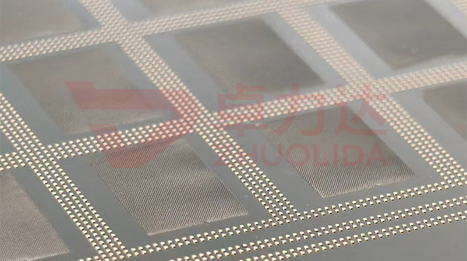
An 8-inch wafer bumping stencil has passed checks at a 30 μm minimum aperture and ±3 μm aperture accuracy, yet ball sizes scatter on the bonder and a few apertures pull a tail. Strip it down and every dimension is in band; the culprit is the slight taper on the aperture wall. Wafer bumping stencil wall taper control governs how the wall opens or closes from the front face to the back: keep a small positive taper and the ball releases toward the wide end, let the angle grow too large and ball volume shifts with the wall so coplanarity drifts, make it a reverse or zero taper and the ball simply jams. Taper is not machined in; development undercut contributes one stretch and electroforming growth another, and the two stack into the final angle. The line holds a 1–3° window and a top-to-bottom difference under 2 μm on a 30 μm aperture — enough to release, not enough to consume the ±3 μm tolerance.
The common trap is treating taper as a by-product of passing dimensional checks. A batch of 30 μm stencils starts losing ball coplanarity by the fifth wafer; apertures are unchanged and position holds ±7 μm, but sectioning shows a reverse taper that traps the ball at the narrow end and draws a tail. Switch development bath lots and two plates from the same artwork differ in taper by over two degrees, so one printer setting fills balls here and skips them there. Worse, taper and roughness tangle together: fine nodules on the wall hold flux on the slope where wiping cannot reach, and apertures clog before service life is spent. None of these show in a routine ±3 μm aperture re-check, which is why wafer bumping stencil wall taper control needs its own station, sampling angle by section or profiler bath by bath rather than waiting for the bonder to alarm.
Parameter Window
• Taper window: 1–3° positive, release direction toward the wide end, reverse taper scrapped
• Top-to-bottom difference: ≤2 μm on a 30 μm aperture, beyond that it eats the ±3 μm tolerance band
• Wall roughness: Ra ≤ 0.01 μm, taper recheck logged separately from Ra, never merged into one item
• Stencil thickness 15–200 μm; thin foils react more strongly to taper in ball volume, run the lower window
• LDI resolution 8 μm/8 μm, double-side alignment ±5 μm; resist sidewall verticality sets taper first
• Current density 1–4 A/dm² in stages, suppressing wall relief from coarse grain
Manufacturing Process (8 Steps)
1. Artwork preparation — master data for the aperture pattern, taper window and release direction flagged for 30 μm zones.
2. Pre-treatment — substrate cleaning and conductive coating, mandrel passivated to keep strike nodules off the wall.
3. Lamination and LDI — exposure at 8 μm/8 μm resolution and ±5 μm double-side alignment; resist sidewall shaped here.
4. Development — control concentration and time; the undercut sets taper and a reverse taper is stopped at this step.
5. Electroforming — staged nickel-cobalt at 1–4 A/dm², growth face adding positive taper without overshoot.
6. Demolding — one-piece release from the wide end; never force a reverse-taper jam and score the wall.
7. Inspection — checker for openings, vision and flash measurement for ±7 μm position, section sampling for angle.
8. Framing and packing — AB adhesive frame, tension set within a 10–55 N band before shipping.
Core Advantages
1. Clean release — hold wafer bumping stencil wall taper control at 1–3° and balls carry no tails, skipped-ball rate falls sharply.
2. Steady ball volume — top-to-bottom difference ≤2 μm tightens lot-to-lot scatter in deposit across a plate.
3. Dimensions intact — taper inside the window keeps ±3 μm aperture tolerance from being consumed by slope.
4. No clogging — positive taper with a Ra ≤ 0.01 μm smooth wall gives flux nothing to cling to.
5. Faults easy to place — taper has its own station, so a development or electroforming drift shows up at once.
6. Traceable — undercut, current band and sampled angle logged per bath, faults traced to a run.
Typical Applications
1. WLP wafer bumping templates for 4–12 inch wafers, where 30 μm apertures are most taper-sensitive.
2. Ball and Flux stencils for ABF substrates, the Ball stencil being fussy about release draft.
3. Mini LED and BGA fine-pitch printing stencils, where small openings make wall share large.
4. Micro-hole screens for semiconductor material grading, where uneven taper shifts dose.
5. Composite stencils with post height or local thickening, whose step walls are harder to taper.
6. Large-format photovoltaic grid stencils, where whole-sheet taper consistency prevents ball drift.
Design and Selection Notes
1. Fix the angle by aperture first. 30 μm takes 1–2°, larger openings can widen to 3°.
2. Do not rush development. A few tenths of a micron extra undercut pushes the angle out of the window.
3. Let the growth face add positive taper, strike current held at the low end of 1–4 A/dm².
4. Release toward the wide end; scrap a reverse-taper plate rather than force it and score the wall.
5. Give taper recheck its own station — a flat-bed checker cannot read wall slope.
6. Set tension within one of the 10–55 N bands, never mix bands in a lot, or ball release will not match.
7. Where local thickening exists, confirm the step-root taper before any rework.
Seen on its own, wafer bumping stencil wall taper control occupies no standalone step: LDI and development shape the resist sidewall, electroforming growth adds another stretch of slope, and the seconds of release prove whether that taper is enough. Pre-treatment, exposure, development, deposition and stripping each own a stretch, and let any one slip and the 1–3° window will not hold, reverse taper or ball-volume drift follows. What is hard on a line is not one plate with a beautiful taper now and then, but a dozen plates from one bath and several consecutive lots sitting in the same angle, top-to-bottom difference and wall Ra band — only then does ±3 μm aperture accuracy mean anything. For orders with a hard requirement on ball coplanarity, fix development time, the staged current-density curve and release direction into the process card at sampling stage and run to that card; it is cheaper than endlessly retuning release speed and wiping at the bonder. On paper wafer bumping stencil wall taper control is a string of angles and tolerances; on the line it is every plate laying down its ball cleanly at the same slope.
Contact:赖先生
Phone:+86 18938693450
Tel:0755-2708-8292
Email:yw9@zldsmt.com
Add:深圳市宝安区福永镇新和村福园一路华发工业园A3栋
 Zhuolida
