Welcome: Shenzhen Zhuolida Electronics Co.TD
Language:
 ∷

∷
∷
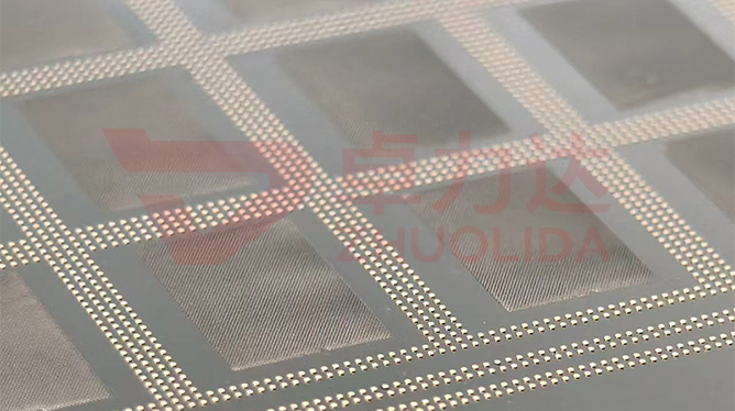
Wafer ball-placement stencil total pitch control is not about whether one aperture sits true; it is about whether the whole coordinate field has drifted by the time you count from the datum hole out to the farthest hole at the panel edge. A WLP stencil carries hundreds of thousands of openings, and holding single-hole position to ±7 μm and aperture to ±3 μm is only a local pass. Compare the measured span between first and last hole along X and Y with the design value and the difference is the total pitch deviation. A spot check never sees it: every hole sits inside its own tolerance circle, yet once errors accumulate in the same direction along the array, by the edge of a 610×660 mm panel an entire row of openings has shifted bodily. The line calls it 'global drift', and this control is what breaks that invisible accumulation down, measures it, and pushes it back.
Three failures show up most often on the floor. One is the stitch seam left by segmented LDI exposure: align each exposure field as well as you like, the two or three microns of mismatch where fields meet still builds outward along the array, and by the panel edge total pitch has crossed ±7 μm — while the sampling points all happen to sit mid-field. Two is the overall scaling brought by large-panel deposition and release: on a 610×660 mm substrate the centre and edge see different bath flow and a two- or three-degree temperature spread, the foil shrinks slightly as nickel stress lets go, the first-to-last span shortens with it, and the outer row of solder balls no longer lands on the pads during placement. Three is dimensional springback after low-temperature anneal that never made it into the data, so a compensation map tuned on the last lot is copied straight onto the next and the deviation reproduces unchanged. A vision gauge sampling a few points catches none of these; unless wafer ball-placement stencil total pitch control measures the three sources separately, they usually surface only after placement, when an entire panel shifts and is scrapped.
Parameter Window
• Total pitch cumulative deviation: ≤±7 μm across the full panel in both X and Y, reported as a per-zone deviation curve over the 610×660 mm format, not a single-point pass.
• Position accuracy ±7 μm, aperture accuracy ±3 μm, minimum opening ≥25 μm — local figures logged and judged separately from total pitch.
• Pitch ≥120 μm, web ≥50 μm; global coordinates zeroed on one corner datum hole, never converted around the panel centre.
• LDI resolution 8 μm/8 μm, double-side alignment ±5 μm; stitching error ≤2 μm per zone before it may accumulate toward the edge.
• Stencil thickness 15–200 μm, tension 10–55 N (±1 N internal line); thin foils are more sensitive to total-pitch shrink from stress.
• Nickel alloy hardness 450–550 Hv, wall roughness ≤0.01 μm; first-to-last span shrink after low-temperature anneal fed into compensation.
Manufacturing Process (8 Steps)
1. Data zoning — split hundreds of thousands of openings into exposure zones across the 610×660 mm format, write a compensation value per zone, one datum hole for all.
2. Substrate pre-treatment — clean and render the large panel conductive, hold flatness and the thermal-expansion datum so no overall scaling enters the coordinates.
3. Lamination and LDI — expose zone by zone at 8 μm/8 μm resolution and ±5 μm double-side alignment, logging the actual stitch coordinate of each seam.
4. Development — verify every zone opens cleanly after development, with attention to the rows beside each seam for resist residue pulling them off.
5. Electroforming — current density 1–4 A/dm² zoned, holding internal stress and thickness spread down so stress shrink does not skew the global field.
6. Release and low-temperature anneal — measure how far the first-to-last span shrank after one-piece release and anneal, and log it against the lot.
7. Zoned re-measurement — vision and flash gauges sweep global coordinates along X and Y zone by zone, producing a deviation curve rather than a bare pass.
8. Compensation write-back — fold measured deviation into the next lot exposure data, then frame at a graded 10–55 N before shipping.
Core Advantages
1. Global control — wafer ball-placement stencil total pitch control judges by total pitch, not a spot check, so whole-field drift has nowhere to hide.
2. Seam convergence — zoned compensation holds LDI stitching to ≤2 μm per zone, so error does not build all the way to the panel edge.
3. Steady placement alignment — the outer row of balls meets the pads, and whole-panel shift scrap at WLP placement drops sharply.
4. Lot traceability — a deviation curve is filed per zone, so anomalies trace back to a specific exposure field, bath run and anneal temperature.
5. Large-panel consistency — several sheets from one 610×660 mm panel share a single compensation model, narrowing centre-to-edge coordinate spread.
6. Downstream fit — anneal shrink already written into the data, so total pitch still holds within ±7 μm after release and framing.
Typical Applications
1. 4–12 inch WLP ball placement, millions of openings and a long array span, most sensitive to global coordinates.
2. ABF substrate Ball and Flux stencils, where a larger panel easily amplifies cumulative deviation.
3. BGA and Mini LED fine-pitch printing stencils, where global alignment decides whole-panel print yield.
4. Large-format photovoltaic grid stencils, where a wider format leans harder on zoned compensation to pull total pitch back.
5. Precision screens for semiconductor material grading, where a long aperture array also needs drift held.
6. Composite stencils with local thickening or posts, where uneven stress more readily pulls a whole-field offset.
Design and Selection Notes
1. Fix the datum hole first. Zero the full field on one corner datum, do not keep converting around the panel centre.
2. The larger the format, the finer the zoning. On 610×660 mm, cut along natural exposure-field boundaries rather than stitching across fields by hand.
3. Measure an extra row of holes on each side of a seam; only ≤2 μm per zone may accumulate, otherwise re-expose on the spot.
4. Zone the current density, do not run one value across the whole panel, or stress shrink will drag the global coordinates with it.
5. Measure the first-to-last span before and after low-temperature anneal, write the difference into the model, do not lean on the last lot.
6. Replace spot checks with zoned sweeps. A vision gauge sampling a few points cannot see total pitch drift; sweep a line along X and Y.
7. Write compensation back per lot, and re-calibrate the datum whenever the substrate batch or bath changes.
Taken on its own, wafer ball-placement stencil total pitch control is less a standalone step than a global audit of exposure, deposition and stress. Zoned exposure keeps each field from accumulating error; zoned current and low-temperature anneal keep the whole panel from scaling; line-by-line zoned re-measurement makes the deviation visible. Miss any one and a single-hole ±7 μm pass will not buy a whole-panel pass. What separates capable lines is rarely whether a few hundred thousand apertures can be made at all, but whether a dozen exposure zones on one large panel close on a single coordinate set. For orders that specify stencil cumulative deviation correction, fix datum position, zone boundaries, anneal shrink and the zoned compensation curve into the process card at sampling stage, then run to that card and write back per lot in production — far cheaper than reworking sheets after placement shifts. That is where wafer ball-placement stencil total pitch control earns its keep: turning something a spot check cannot see into a re-measurable, traceable whole-panel coordinate.
Contact:赖先生
Phone:+86 18938693450
Tel:0755-2708-8292
Email:yw9@zldsmt.com
Add:深圳市宝安区福永镇新和村福园一路华发工业园A3栋
 Zhuolida
