Welcome: Shenzhen Zhuolida Electronics Co.TD
Language:
 ∷

∷
∷
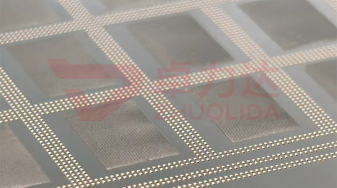
On a mixed assembly board the large QFN pad needs plenty of solder while the 01005 fine pitch needs little but precise — one uniform-thickness stencil cannot serve both, which is why step stencils exist: the body stays a 15–30μm thin web and the Post region over large pads or support points is built up locally to 50–200μm. Where the two thicknesses meet is the step, and its root is exactly where developer pools, tension lifts the sheet, and demolding tears it. Electroformed step stencil local thickening works by zoned deposition: plate the whole sheet to thin-web thickness first, open a window over the buildup zone with a second lamination, then plate that region up to the target class, with the thickness difference set by plating time rather than shims or glue dots. It is a separate ledger from aperture accuracy ±3μm and position accuracy ±7μm.
Build the step badly and every failure grows along that ring of transition. One lot of Post stencils printed pads near the step with solder volume swinging high and low; stripping showed a bead of developer residue pressed into the step root, smearing half the release face of the neighboring aperture. In a bath run at higher current density, the second buildup crowded current at the step edge and grew a dense crop of nodules — aperture remeasurement still sat inside ±3μm, but the walls grabbed paste badly. Tension was worse: cut the transition from buildup to thin web too steep and the sheet lifted from the step root the moment it hit 40N, cracking along the boundary after a few prints. A full stencil checker measures aperture outlines; it cannot read internal stress or residue at a thickness jump. Electroformed step stencil local thickening is hard precisely because of this ring, and by the time it shows up the whole lot is usually scrap.
Parameter Window
• Thin web 15–30μm; buildup region 50–200μm by pad demand
• Step transition width ≥0.3mm internal, to avoid stress concentration at the thickness jump
• Minimum aperture ≥25μm, pitch ≥120μm, web ≥50μm; the step zone checked on its own
• Aperture accuracy ±3μm, position accuracy ±7μm, measured before and after buildup
• Current density 1–4A/dm², held at the low end at the step edge to suppress nodules
• Tension 10–55N (±1N internal), stepped stencils kept in the middle-low band against lifting
Manufacturing Process (8 Steps)
1. Data and drawing — split the thin web and Post buildup zones from the pad map, put the step line on its own layer.
2. Pretreatment — clean and conductivize the base, passivate the mandrel face so the whole sheet starts evenly.
3. Lamination and LDI — 8μm/8μm resolution, double-side alignment ±5μm; first pattern the whole thin layer.
4. Developing — develop the thin layer to define apertures, leave no residue at the step boundary and no undercut.
5. Electroforming — plate the whole sheet to thin-web thickness first, then a second lamination plates the Post region locally, current density 1–4A/dm² in stages.
6. Demolding — peel the whole sheet from a low-stress corner, with the demold direction kept off the step root.
7. Inspection — checker measures apertures, imager and flash gauge verify positions, a thickness gauge sweeps the step transition.
8. Mounting and packing — aluminum frame bonded with AB adhesive, tension set in the 10–55N middle-low band before shipment.
Core Advantages
1. Two thicknesses in one sheet — stable electroformed step stencil local thickening lets large pads and fine pitch each get what they need.
2. One fewer bond — no extra thin web to laminate or glue to build up, so a shorter process and one less alignment error.
3. Controlled step — transition width and thickness difference fixed in the process card, matching lot to lot.
4. Size and thickness managed apart — ±3μm goes to the checker, step thickness to the thickness gauge.
5. Steadier demolding — direction kept off the step root, no collapsed mouths and no paste grab.
6. Traceable — each zone logs first and second plating time and current class for bath-run lookup.
Typical Applications
1. QFN and module mixed-assembly stencils, large pads and fine pitch printed on one board.
2. 4–12 inch WLP ball-drop templates, local buildup holding solder ball volume.
3. ABF substrate Ball and Flux plates, Post buildup controlling deposit volume.
4. Precision sieves for semiconductor material classification, local buildup serving as stiffeners.
5. Composite plates with locating posts or support blocks, the step structure being the same family.
6. Large-format grids such as photovoltaic stencils, local buildup resisting squeegee downforce.
Design and Selection Notes
1. Set thickness class from the pad first — hold the thin web at 15–30μm, do not pile the buildup upward blindly.
2. Do not cut the step transition too steep — too narrow and tension lifts it from the root.
3. Watch second lamination alignment closely — double-side alignment ±5μm, a little error and the step lands on an aperture.
4. Hold current at the low end at the step edge — 1–2A/dm² slow deposition, fewer nodules and cleaner walls.
5. Keep the demold direction off the step root, the ring most easily torn.
6. Sweep the full width of local thickening stencil thickness transition with a thickness gauge, not just one center point.
7. Keep stepped stencils in the 10–55N middle-low band and never mix classes in one lot.
Taken down to operations, electroformed step stencil local thickening simply splits one electroforming run into two: a whole thin layer fixes the apertures first, a second lamination opens a window only over the Post region to build it up, and how flat or steep the step is comes down entirely to alignment and developing between those two runs. Pretreatment, first exposure, second exposure, two deposition stages and peeling each guard one stretch, and if any drifts, thickness difference and transition width run together. What is hard is not producing one sample with two crisp classes, but keeping a dozen sheets from one bath and several consecutive lots free of pooled residue, lifting and paste grab at the step root — only then does ±3μm aperture accuracy match before and after buildup. For orders with hard mixed-assembly requirements, fix thin-web target thickness, second buildup time, step transition width and demold direction in the process card at the sampling stage and run production to it; that is far cheaper than shimming flat and endlessly adjusting squeegee pressure at the printer. On paper electroformed step stencil local thickening is two thickness classes; on the line it is that ring of step staying clean and flat every time.
Contact:赖先生
Phone:+86 18938693450
Tel:0755-2708-8292
Email:yw9@zldsmt.com
Add:深圳市宝安区福永镇新和村福园一路华发工业园A3栋
 Zhuolida
