Welcome: Shenzhen Zhuolida Electronics Co.TD
Language:
 ∷

∷
∷
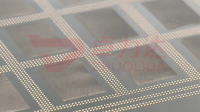
Take a 40 μm printing stencil: the floors of its several hundred thousand apertures are already clean and aperture accuracy of ±3 μm has been measured, yet what really sets print performance is the invisible texture on the aperture sidewalls. Precision electroformed stencil wall roughness control governs the microscopic relief left when nickel is copied from the resist sidewall onto the metal wall — how coarse the grain is, whether nodules have grown, whether resist residue turns into pits. It never appears in the aperture dimensions, but it decides whether paste drops as one plug or drags a tail on release. Wall roughness is normally quoted as Ra, and the delivery line here is ≤ 0.01 μm, an order of magnitude below the finish of many machined parts. It is not achieved by downstream polishing, which a thin foil cannot survive, but by fixing the conditions at the moment of deposition.
The common trap on the line is treating wall roughness as a cosmetic issue. A fine-pitch Mini LED stencil starts bridging on the third board; strip it down and the aperture size is unchanged and position is true, but side-lighting under a vision system shows a film of paste clinging to the wall that will not wipe off. Switch to another bath lot and the same stencil lays down uneven volumes across BGA pads; section it and the wall is dotted with fine nodules that trap paste in the hollows and slow the release. More subtle still: overdose the brightener and the grain refines and hardness climbs to 550 Hv, yet the wall grows striations along the current lines, release drag rises with them, and burrs appear at the aperture rim after a few thousand prints. None of these failures show up in a ±3 μm aperture re-check, and by the time they surface a whole batch of substrates is usually scrap. Stencil wall roughness measurement therefore cannot rely on a flat-bed checker scanning openings; the sidewall has to be measured on its own, which is why precision electroformed stencil wall roughness control is harder to put into practice than dimensional inspection.
Parameter Window
• Wall roughness: Ra ≤ 0.01 μm as the delivery ceiling, held to 0.008 μm internally for margin
• Bath current density: 1–4 A/dm², fine-pitch apertures run at the lower end for slow deposition
• Stencil thickness: 15–200 μm; foils under 30 μm react more strongly to sidewall texture
• Minimum aperture ≥25 μm, pitch ≥120 μm, web ≥50 μm; wall area grows as a share of the opening as apertures shrink
• Aperture accuracy ±3 μm and position accuracy ±7 μm, re-checked separately from wall condition
• Nickel alloy hardness 450–550 Hv; when hardness comes from grain refinement, watch internal stress alongside it
Manufacturing Process (8 Steps)
1. Artwork preparation — master data for the aperture pattern, with sidewall requirements flagged for fine-pitch zones.
2. Pre-treatment — substrate cleaning and conductive coating, plus low-adhesion passivation of the mandrel to avoid strike nodules.
3. Lamination and LDI — imported LDI exposure at 8 μm/8 μm resolution and ±5 μm double-side alignment; resist sidewall verticality is set here.
4. Development — control developer concentration and time so no residue stays at the foot and the sidewall is not undercut; the first wall profile is decided here.
5. Electroforming — staged control of current density at 1–4 A/dm² and bath temperature suppresses coarse grain and nodules while wall thickness is watched as it grows.
6. Demolding — one-piece release from a low-stress corner; the wall is most easily scored at the instant of lift-off.
7. Inspection — automatic stencil checker for openings, vision and flash measurement for position, white-light profiler sampling wall Ra.
8. Framing and packing — aluminium frame bonded with AB adhesive, tension set within a 10–55 N band before shipping.
Core Advantages
1. Clean release — hold precision electroformed stencil wall roughness control at Ra ≤ 0.01 μm and paste transfers as one plug, with bridging at fine pitch falling off sharply.
2. Stable deposit volume — no nodules or pits on the wall, so paste release from a given opening varies less from lot to lot.
3. No polishing — thin foils skip downstream mechanical buffing, so 15–30 μm sheets do not distort or collapse at the rim.
4. Dimensions and surface tracked apart — ±3 μm aperture accuracy belongs to the checker, wall condition to the profiler, so a fault can be pinned to a bath run.
5. Truer service life — a smooth wall holds less paste, so decay is slower as print life approaches 15,000 cycles.
6. Traceable — current density, brightener dosing and sampled Ra are logged per bath, so a problem reaches back to the solution lot.
Typical Applications
1. Mini LED and BGA fine-pitch printing stencils, where small openings are most sensitive to paste clinging to the wall.
2. WLP ball-placement templates for 4–12 inch wafers, where millions of openings demand uniform release.
3. Ball and Flux stencils for ABF substrates, the Ball stencil being especially fussy about wall release.
4. Precision screens for semiconductor material grading, where clean micro-hole walls resist clogging.
5. Composite stencils with post height or local thickening, whose step sidewalls retain texture more readily.
6. Large-format photovoltaic grid stencils, where wall uniformity under a long squeegee stroke sets whole-sheet consistency.
Design and Selection Notes
1. Fix the current band by pitch first. Conventional spacing at ≥120 μm can run the upper end; fine pitch always takes 1–2 A/dm² slow deposition.
2. Under-dose the brightener rather than over-dose it. At 550 Hv the grain is fine, but wall striations and internal stress arrive together.
3. Do not rush development. A few tenths of a micron of undercut becomes a permanent step on the nickel wall.
4. Verify mandrel passivation per lot; nodules tend to start where the conductive layer is uneven.
5. Give stencil wall roughness measurement its own station — a flat-bed checker cannot read sidewall Ra, so set the sampling rate per lot.
6. Set tension within one of the 10–55 N bands and never mix bands in a lot, or paste release behaviour will not match.
7. Where local thickening exists, choose a release direction that avoids the step root, the spot most easily scored.
Seen on its own, precision electroformed stencil wall roughness control barely occupies a standalone step: the resist sidewall is shaped by LDI and development, the grain grows as it will in the bath, and the few seconds of release decide whether that texture survives intact. Pre-treatment, exposure, deposition and stripping each own a stretch of it, and let any one slip and the ≤ 0.01 μm line will not hold. What is genuinely hard on a line is not turning out one clean sheet now and then, but keeping a dozen sheets from one bath and several consecutive lots inside the same wall band — only then does ±3 μm aperture accuracy mean anything. For orders with a hard requirement on sidewall release, fix current density, the brightener dosing curve and development time into the process card at sampling stage and run to that card in production; it is far cheaper than endlessly retuning release speed, wiping the stencil and swapping paste at the printer. On paper precision electroformed stencil wall roughness control is a string of parameters; on the line it is the simple fact that every sheet lays down its paste cleanly in the same state.
Contact:赖先生
Phone:+86 18938693450
Tel:0755-2708-8292
Email:yw9@zldsmt.com
Add:深圳市宝安区福永镇新和村福园一路华发工业园A3栋
 Zhuolida
