Welcome: Shenzhen Zhuolida Electronics Co.TD
Language:
 ∷

∷
∷
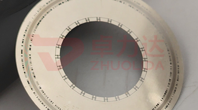
Glass through via (TGV) electroforming is a process that forms micro-holes in ultra-thin glass substrates and then fills them completely with copper, building vertical metal interconnect paths that run from the top surface to the bottom. It takes a different route from silicon TSV: silicon through-holes are first opened by deep reactive ion etching and then plated with copper, whereas glass through-holes are drilled in the glass first and then copper is grown to pack the cavity by electroforming. Glass has a coefficient of thermal expansion closer to that of copper wiring layers, a lower high-frequency dielectric loss, and can be made into panels larger than silicon wafers, which matters for interposers that must balance low loss with large format. For packaging houses chasing high-density routing and low signal loss, this step decides whether a glass substrate can move from sample to volume, and whether panel-level packaging can actually bring costs down.
In 2.5D/3D and panel-level packaging, interconnect density keeps climbing every year, and conventional silicon TSV is starting to run out of headroom. The thermal-expansion gap between silicon and copper is fixed, and the deeper the hole and the larger the panel, the higher the risk of warpage and stress cracking, with large-format interposers especially exposed. Silicon is also a semiconductor substrate whose dielectric loss and parasitic effects at high frequency cannot be suppressed, which hurts radio-frequency front ends, millimeter-wave, and optical-communication scenarios in particular. The real difficulty of glass through-holes lands on the fill step: holes only 20 to 30 µm wide with aspect ratios of ten to one are easy to leave gaps or voids at the center under ordinary plating, and once a via is discontinuous the entire interconnect is scrap. Electroforming fill pushes copper uniformly from the wall toward the center with pulse current and a high-throwing-power electrolyte, achieving void-free full fill and a flattened surface, which is exactly what gives glass substrates real production value. In short, fill quality is the gateway to TGV yield, and the dividing line between glass and silicon interposers.
Parameter Window
• Glass substrate thickness: 0.1–1.0 mm (100–1000 µm), selectable by package tier
• Via diameter: 20–100 µm, aspect ratio up to 10:1
• Fill metal: oxygen-free copper, bulk resistivity about 1.7 µΩ·cm
• Fill quality: void-free full fill, no center cracks, no trapped gas
• Warpage control: full-panel warpage < 50 µm, better than same-size silicon
• Post-processing: anneal for stress relief, CMP planarization, double-side exposure
Manufacturing Process (8 Steps)
1. Glass hole opening — laser, sandblast, or wet etch forms the through-holes, controlling taper and wall quality.
2. Seed-layer preparation — sputter a thin Ti/Cu layer as a conductive base for uniform, continuous coverage.
3. Photolithography patterning — coat and develop resist to define fill and routing areas, protecting non-via regions from plating.
4. Pulse electroforming fill (core step) — pulse current deposits copper from wall to center inside the hole, filling it without voids.
5. Anneal stress relief — heat treatment relaxes the copper-glass interface stress and suppresses later warpage and delamination.
6. CMP planarization — grind away excess surface copper so the via mouth is flush with the substrate for upper-layer routing.
7. Double-side exposure and RDL — expose copper posts on both faces and build redistribution lines for top-bottom interconnect.
8. Inspection and test — microscope and electrical test verify via continuity, resistance, and warpage before release.
Core Advantages
1. Low-loss interconnect — glass loss tangent far below silicon, cleaner RF and optical signals, easier to extend high-speed links.
2. Low-warpage large format — glass and copper match thermally, so large-panel warpage is controllable and yield beats same-size silicon interposers.
3. Void-free full fill — pulse electroforming packs the hole solid, avoiding interconnect breakage from voids and lifting reliability.
4. High-frequency merit — fits millimeter-wave, CPO co-packaging, and high-speed SerDes where parasitic effects are smaller.
5. Cost and large panel — glass substrates can be made as large panels, per-interconnect cost below silicon interposers, friendly to volume.
6. Process compatibility — links cleanly with existing RDL, micro-bump, and fan-out processes; change artwork without changing hard tooling, iterate fast.
Typical Applications
• 2.5D/3D packaging interposers — glass transponders link logic chips and HBM, cutting interconnect loss and crosstalk.
• RF front-end modules — millimeter-wave antennas and power-split networks use glass low loss to lift transceive efficiency.
• Co-packaged optics (CPO) — high-speed optical engines and electrical chips interconnected near-package with better signal integrity.
• Sensors and MEMS — through electrodes and suspended structures; glass insulates and stays thermally stable for harsh environments.
• Power and automotive — high-current vertical interconnect; glass temperature and insulation fit automotive-grade reliability.
• Advanced substrate replacement — partially replaces silicon interposers, easing silicon supply tightness and cost pressure.
Design and Selection Points
1. Via diameter and aspect ratio must match electroforming fill capability; reserve pulse parameters for deep holes.
2. Seed-layer coverage must be continuous; broken seed at the wall directly fails fill, so strengthen pre-treatment.
3. Glass type (fused silica / borosilicate / soda-lime) trades off loss and cost; pick low-loss glass for high frequency.
4. Must anneal and CMP after fill; unplanarized surfaces hurt upper RDL alignment accuracy.
5. Large panels need whole-panel warpage control; validate small batches before scaling to panel level to avoid total scrap.
6. Via and routing compensation must account for plating uniformity; densify seed and lower current at edge holes.
7. When co-designing with fan-out and micro-bump, unify the metallization system to avoid interface mismatch and peeling.
Glass through via electroforming fill has become the mainstream interconnect scheme for glass substrate packaging because it packs micro-holes solid with copper, delivering interconnect density close to silicon interposers on low-cost glass while holding down high-frequency loss and warpage. As panel-level packaging and CPO co-packaging raise demand for large-format, low-loss interconnects, the value of glass through via electroforming fill will grow further in 2.5D/3D and RF scenarios. Choosing glass through via electroforming fill essentially locks in three gains at the interconnect stage: low loss, low warpage, and high yield. That is also the fundamental difference from conventional silicon TSV. As packaging density and signal rates keep climbing, securing interconnect continuity from the fill step is often more certain than remediation downstream, and better supports the quality floor and long-term customer trust of advanced-packaging volume ramp-ups.
Contact:赖先生
Phone:+86 18938693450
Tel:0755-2708-8292
Email:yw9@zldsmt.com
Add:深圳市宝安区福永镇新和村福园一路华发工业园A3栋
 Zhuolida