Welcome: Shenzhen Zhuolida Electronics Co.TD
Language:
 ∷

∷
∷
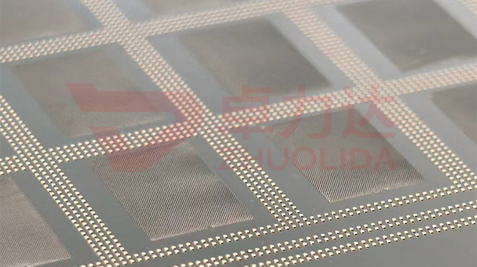
What an optical aperture fears most is not an oversized or undersized hole, but an unclean corner. The clear openings on the drawing are crisp right angles; round that corner on the finished part, even by an R of only two or three microns, and the edge-diffraction and stray-light boundary move with it, showing up as a soft ring in high-contrast imaging. Aperture development pattern fidelity governs how that contour travels from photoresist into the nickel without distortion: LDI drawing the pattern in resist is only the start, and whether development swells the resist wall, whether post-bake lets the corner reflow into a curve, whether strike fills the right angle into a small arc — every step reshapes the contour. Line width measures a dimension, fidelity looks at shape; a 20 μm rib can pass on width yet fail on installation because its corners are round. Contour comparison, put plainly, takes the right angle on the master as the datum and overlays the figure after every step to see whether the corner is still there.
Contour failures often only show up under magnification. One lot of aperture plates passed every width check, yet a vision system at high power found a short arc at all four corners of each square opening: post-bake temperature had been set too high, the photoresist reflowed slightly at the corners, and nickel grew to that curve, losing the right angle. Another lot was subtler: a flash system read the openings fine, but a point light source gained a halo once installed; the cause was laminated LDI exposure that had not aligned both sides within ±5 μm, leaving a slight slope in the resist sidewall that electroforming faithfully carried into the nickel wall, so the contour was no longer the straight up-and-down face in the design. Then there is mandrel reuse: an old plate carrying resist residue at a corner puts an R corner at the same spot on every later part, and aperture development pattern fidelity gets dragged down by a bit of dirt on the plate. A calliper cannot find these; only contour comparison brings them out. That haloed lot was remade later, with post-bake temperature pulled down and development time pinned, and the halo cleared only on the next mounting — a detour far costlier than one extra contour pass.
Parameter Window
• Aperture rib and line width 20 μm, corner R held near zero internally, contour comparison per part
• LDI resolution 8 μm/8 μm and ±5 μm double-side alignment; a vertical resist sidewall is the premise of fidelity
• Maximum substrate 610×660 mm; exposure uniformity across the panel decides whether corner radius is consistent everywhere
• Development time and post-bake temperature fixed per band; over-bake reflows corners, under-development leaves residue
• Bath current density 1–4 A/dm²; a strike stage set too high fills the right angle into an arc first
• Aperture accuracy ±3 μm and aperture wall roughness ≤0.01 μm; only a smooth straight wall can be called contour-true
Manufacturing Process (8 Steps)
1. Artwork and compensation — release master data to an R-corner-free requirement, no automatic corner rounding, with fidelity zones marked separately.
2. Mandrel check — inspect corners for resist residue and scratches on a vision system before plating, and cap reuse count for old plates.
3. Lamination and LDI — imported LDI exposure at 8 μm/8 μm, ±5 μm double-side alignment, layout on a 610×660 mm panel.
4. Development for shape — pin development time and post-bake temperature to keep walls vertical and corners sharp, with no base film left behind.
5. Contour review — measure the resist pattern's corners right after development and roll back if the radius is out, rather than finding it after electroforming.
6. Low-current strike — lay a thin nickel film along the resist contour at low current, locking the right angle before normal deposition.
7. Release and anneal — peel the whole part from a low-stress corner and low-temperature anneal so the contour does not spring back.
8. Finished-part comparison — vision and flash systems overlay the nickel contour on the master data and grade by R corner and width together.
Core Advantages
1. Right angles survive — shape-setting development plus low-current strike leaves no visible R corner from resist to nickel.
2. Optical boundary is true — stray-light suppression and diffraction match design, with no halo around a point source.
3. Problems move upstream — resist contour is reviewed after development, so rounding is stopped before the part enters the bath.
4. Consistent across the panel — shared exposure and development conditions on 610×660 mm keep corner radius in one band everywhere.
5. Old plates stop being the excuse — corner residue and reuse count are controlled, so aperture development pattern fidelity does not slide with plate revision.
6. Traceable — master ID, development conditions and contour overlay are logged per part, so anomalies trace back to the plate.
Typical Applications
1. Camera module and imaging objective apertures, where square right angles set the stray-light boundary and edge sharpness directly.
2. Field stops in lithography and inspection tools, where an R corner rounds off the corners of the usable field.
3. Medical endoscope and microscopy aperture plates, where dense small square holes are most sensitive to corner fidelity.
4. Laser shaping and grating masking plates, where a rounded contour drops fringe contrast with it.
5. Star-tracker and aerospace stray-light suppression plates, which rely on right-angle contours to hold down edge diffraction.
6. Research shaped-aperture arrays, where non-standard corners are many and contour comparison matters more than dimension checks.
Design and Selection Notes
1. Write the R-corner-free requirement into the drawing. Mark only width and aperture and the supplier will round corners by default.
2. Verify development and post-bake together. Straight resist walls with over-bake reflow still turn the right angle round in nickel.
3. Beyond ±5 μm double-side alignment, check resist sidewall slope; a slope carried into nickel is contour distortion.
4. Do not rush the strike current. Set the first nickel layer too high and the right angle is filled round before anything later can fix it.
5. Set a reuse limit for the mandrel. Once residue builds at a corner, every later part carries an R corner at that same spot.
6. Accept with a contour overlay. Dimension checks cannot see a radius; overlay the finished contour back onto the master data.
7. On shaped parts, set the development window by the sharpest corner, not by an average width applied to every corner.
Laid out, aperture development pattern fidelity is not about whether the openings are cut accurately, but whether that right-angle contour has been quietly altered somewhere between photoresist, nickel layer and master plate. Laminated LDI draws it straight, shape-setting development keeps the resist corner from reflowing, and low-current strike keeps nickel from filling the right angle round. Miss any one and the finished part carries an R corner whose origin is hard to name, and passing width will not bring it back. What separates capable lines is rarely how pretty one contour is, but whether a dozen parts on a 610×660 mm panel, across several master changes, still share the same crisp corner. For orders that specify electroformed aperture contour transfer, fix the master ID, post-bake condition and contour comparison method into the process card at sampling stage and ship with the overlay record — far more reliable than picking parts by halo under a point light after mounting. That is where aperture development pattern fidelity lands: turning shape, which cannot be measured with a calliper, into a deliverable that can be overlaid and traced.
Contact:赖先生
Phone:+86 18938693450
Tel:0755-2708-8292
Email:yw9@zldsmt.com
Add:深圳市宝安区福永镇新和村福园一路华发工业园A3栋
 Zhuolida
