Welcome: Shenzhen Zhuolida Electronics Co.TD
Language:
 ∷

∷
∷
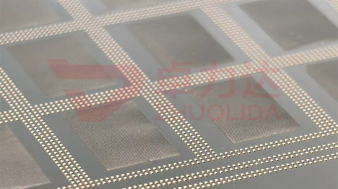
In an aperture seated inside an imaging objective, only a 20 μm nickel rib stands between the clear openings to block stray light. Make that rib wider and it eats into the clear area, shifting edge diffraction with it; make it narrower and it snaps at release or cleaning, scrapping the whole part. Aperture rib and line width forming control watches that 20 μm all the way from resist pattern to nickel rib: drawing the line in resist by exposure is one thing, whether development leaves the resist wall straight and whether nickel grows sideways along that wall during electroforming is another. Nickel grows against the resist pattern, so a slightly higher current or a slightly longer run fattens the rib past the resist outline; once the width-to-depth ratio changes, mechanical strength and the optical boundary both move. What is controlled here is not the number read off one line, but whether line width still tracks the design value once the development and deposition windows are stacked together. Lines tend to clamp the two stages separately, yet the resist wall and the nickel wall grow as one connected mould; slip half a step in the middle and the finished part cannot be brought back.
Trouble on fine ribs comes from those windows drifting apart. One batch got a few seconds too many in development, undercutting a slight taper at the resist wall base; the resist pattern still measured fine on a vision system, yet after electroforming the nickel rib bulged at its root and 20 μm read closer to 23 μm, so the installed clear aperture ran small and the image corners went dark. Another batch went the other way: over-development thinned the resist wall, nickel crept sideways fast at strike, and a flash scan found ribs from 18 μm to 24 μm on one part — the cause was higher current density at the edge of a 610×660 mm panel, so the outer parts fattened first. The worst case is rib breakage: a lot looked intact after release but came out of ultrasonic cleaning short of three or four ribs, because deposition current had been held below 1 A/dm², leaving a loose deposit that never made the 20 μm rib solid. When aperture rib and line width forming control does not tune development and deposition together, this kind of spread keeps coming back. Later, development time and stop time were tied onto one card and adjusted as a pair, and only then did the outer parts' widths pull back into the same band.
Parameter Window
• Aperture rib and line width 20 μm, deviation held at micron level internally, re-measured per part on a vision system
• LDI resolution 8 μm/8 μm and ±5 μm double-side alignment; the resist line width is where forming starts
• Maximum substrate 610×660 mm; only edge shielding holds down the current crowding at the panel rim
• Bath current density 1–4 A/dm²; fine-rib parts favour the 2–3 A/dm² middle, where growth is steady and gain small
• Aperture wall roughness ≤0.01 μm and aperture accuracy ±3 μm; a smooth sidewall is what keeps resist residue off
• Nickel alloy hardness 450–550 Hv; hard enough to stand, too hard turns brittle and snaps in cleaning
Manufacturing Process (8 Steps)
1. Artwork release — set rib width and layout from the clear aperture, mark compensation at fine ribs separately, and do not reuse standard stencil data.
2. Substrate pre-treatment — degrease and activate the mandrel, lay an even conductive layer so a 20 μm resist rib has a surface to grip.
3. Lamination and LDI — imported LDI exposure at 8 μm/8 μm, ±5 μm double-side alignment, layout on a 610×660 mm panel.
4. Development for straight walls — pin down development time and post-bake temperature, keep walls straight and base film clear, and roll parameters back the moment a taper appears.
5. Low-current strike — lay a thin nickel film along the resist rib at low current to lock the width, then enter normal deposition so the strike stage does not creep sideways.
6. Staged electroforming — feed 1–4 A/dm² by zone with edge shielding, and compute stop time from target thickness so fine ribs do not fatten.
7. Release and anneal — peel the whole part from a low-stress corner and low-temperature anneal, so fine ribs neither spring back nor bow.
8. Line-width re-test — vision and flash measurement for rib width and aperture wall per part, graded by width deviation and shipped with the re-test record.
Core Advantages
1. Width tracks design — straight-wall development plus width-locking strike keeps lateral gain on a 20 μm rib at micron level from resist to nickel.
2. Clear aperture is right — ribs neither fat nor thin, so image edges stay bright and diffraction matches design.
3. Fine ribs do not snap — mid-band current density makes the deposit solid, so no missing ribs or flakes after ultrasonic cleaning.
4. Consistent across the panel — edge shielding on 610×660 mm keeps outer and centre parts in one width band.
5. Thin and thick parts both fit — the same aperture rib and line width forming control sets stop time by thickness rather than picking its jobs.
6. Traceable — development time, current curve and width re-test are logged per part, so anomalies trace back to the exposure plate.
Typical Applications
1. Imaging objective and camera module apertures, where a 20 μm rib blocks stray light and its width sets the clear aperture directly.
2. Field stops in lithography and inspection tools, where a rib a touch too fat shaves a strip off the usable field.
3. Medical endoscope and microscopy aperture plates, dense with fine ribs and cleaned often, where one break scraps the part.
4. Laser processing and grating encoder masking plates, where rib-width consistency drives fringe contrast.
5. Stray-light suppression plates in aerospace and automotive optics, where wide temperature swings demand width that does not drift with stress.
6. Research multi-step aperture arrays, where several rib widths share one part and the window must be set by the finest of them.
Design and Selection Notes
1. Fix the clear aperture before the rib width. Do not hand over a lone 20 μm number; write down tolerance and compensation direction.
2. Tune development and deposition together. Straight resist walls with high current still let nickel grow sideways; watching one stage alone does nothing.
3. Shield the panel edge. Current crowds at the rim of 610×660 mm, and fine ribs run widest there.
4. Do not push current below 1 A/dm² chasing thin ribs. A loose deposit means a 20 μm rib snaps in cleaning.
5. The ±5 μm double-side figure belongs to exposure; post-release width re-measurement is the delivery figure.
6. For orders with ultrasonic cleaning, write rib strength into acceptance; width measurement alone cannot see brittle-fracture risk.
7. When several rib widths coexist, set development and stop-time windows by the finest one, not by an average width.
Seen on its own, aperture rib and line width forming control is not the reading of one step but how much of that 20 μm line survives once the development and deposition windows are stacked. Straight-wall development keeps the resist from tapering, low-current strike locks width first, and zoned feed stops nickel growing an extra sliver at the edge. Miss any one and the finished rib quietly fattens by a few microns, and the clear aperture shifts with it. What separates capable lines is rarely whether 20 μm can be made at all, but whether a dozen parts on a 610×660 mm panel, across several lots, all sit on the same width. For orders that specify electroformed aperture fine-rib replication, fix development time, post-bake temperature and stop time into the process card at sampling stage and keep per-part width records — far easier than picking out broken ribs after cleaning. That is where aperture rib and line width forming control lands: merging two windows into one repeatable parameter band.
Contact:赖先生
Phone:+86 18938693450
Tel:0755-2708-8292
Email:yw9@zldsmt.com
Add:深圳市宝安区福永镇新和村福园一路华发工业园A3栋
 Zhuolida
