Welcome: Shenzhen Zhuolida Electronics Co.TD
Language:
 ∷

∷
∷
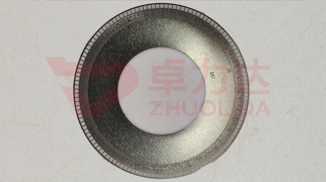
People who make grading screens look at holes differently from people who make printing stencils: a stencil is judged by opening size and wall finish, a screen is judged first by whether the hole is truly round. A single electroformed screen carries hundreds of thousands of round holes, and a few microns of difference between long and short axis lets a particle that should be retained slip through the long way, broadening the size distribution at once. Electroformed screen roundness control governs exactly that — from the circular pattern drawn by LDI, through the resist pillar sidewall after development, to the nickel rim once the layer has grown, roundness has to survive every stage, with a delivery line of ±0.002 mm, or ±2 μm. That figure is tighter than the ±3 μm aperture tolerance, which means hole shape has to be measured as its own metric and not quietly folded into a pass or fail on aperture size. On semiconductor material grading and pharmaceutical powder screening, customers accept against a cut-off curve, and an out-of-round hole makes that curve ugly.
Anyone burned on the line remembers a few signature failures. One lot re-measured entirely inside ±3 μm on aperture yet still cross-graded on the sizing run; fitting the holes under a vision system showed the long axis 3 μm over the short, with the long axis in tolerance and the short one out — a single-aperture check simply cannot report that. Change the bath and a small tail grows on one side of the rim, pulling round holes into pear shapes; trace it back and the current shield is dense at the edge and thin at the centre, so nickel grows faster on one side along the field lines. Then there is the old large-panel problem: on a 610×660 mm substrate the edge holes are round while a central patch goes slightly oval, whole-sheet shape consistency suffers, and the cut point shifts by half a band from one area of the same screen to another. None of these live in the aperture data, and none can be corrected afterwards — once the nickel has grown, the shape is set. Electroformed screen roundness control can only be pushed upstream, onto the exposure pattern, development conditions and current distribution.
Parameter Window
• Screen roundness ±0.002 mm (±2 μm) as the delivery ceiling, held to ±0.0015 mm internally
• Micro-hole aperture tolerance ±3 μm, with long and short axes measured and judged separately
• Minimum aperture ≥25 μm, web ≥50 μm, pitch ≥120 μm; roundness gets harder as holes shrink
• LDI resolution 8 μm/8 μm and ±5 μm double-side alignment; circular pattern fidelity is set here
• Bath current density 1–4 A/dm²; whole-panel current uniformity decides whether rims grow off-centre
• Substrates up to 610×660 mm, with edge-to-centre shape difference converged region by region
Manufacturing Process (8 Steps)
1. Circular artwork — build the hole array from the target particle size and flag the roundness-critical zones.
2. Substrate pre-treatment — clean and make conductive, passivate the mandrel for low adhesion so strike nodules do not skew the rim.
3. Lamination and LDI — imported LDI exposes the round-hole array at 8 μm/8 μm resolution and ±5 μm double-side alignment.
4. Development — hold conditions so resist pillars stand vertical, neither collapsing nor widening; hole shape is first preserved here.
5. Electroforming — even flow across the panel, current density staged at 1–4 A/dm² to stop one-sided growth.
6. Demolding — one-piece release, with no tearing or pulling that would distort the thin walls of round holes.
7. Shape inspection — vision and flash systems fit roundness region by region, while the checker tallies long-to-short axis spread and consistency.
8. Grading trial — run a standard particle-size sample through the screen, confirm the cut point, then certify and ship.
Core Advantages
1. Accurate cut — long-to-short spread held within ±2 μm gives a sharp cut point and no cross-grading.
2. Consistent shape — whole-panel regional fitting puts edge and centre inside the same roundness band.
3. No rework — roundness is formed upstream in one pass, with no downstream correction after the nickel has grown.
4. Data separable — long axis, short axis and roundness archived apart, so a fault pins to an exposure zone or a bath run.
5. Trial-backed — a standard particle-size pass before shipping keeps geometry and grading behaviour in agreement.
6. Traceable lots — electroformed screen roundness control files exposure compensation, current distribution and trial-sieve records together.
Typical Applications
1. Semiconductor material grading, where the particle cut point is most sensitive to hole shape.
2. Pharmaceutical powder screening, where round-hole consistency affects particle-distribution compliance.
3. Fine chemical filtration, where an out-of-round hole creates a local excess of flow.
4. Precision micro-hole screens, where roundness on ≥25 μm holes is especially tight.
5. Standard and calibration sieves, where roundness tolerance is itself an acceptance item.
6. Large-format grids, where whole-panel shape consistency on 610×660 mm sheets is the delivery challenge.
Design and Selection Notes
1. Set aperture from the target particle size, then set the roundness band separately; do not let a ±3 μm aperture tolerance quietly govern hole shape.
2. Give roundness its own inspection station. A checker reading one aperture value cannot report long-to-short spread; regional fitting is what counts.
3. Leave compensation in the artwork. Circular arrays drift systematically through LDI and development, so fine-tune against per-lot re-measurement.
4. Do not over-develop. A resist pillar that slumps or widens becomes a permanent oval in the nickel.
5. Match shields and racks to panel width; beyond 1–4 A/dm², watch whole-panel current spread, since fast edge growth always skews holes.
6. Measure and log both axes, and compute yield over hole count rather than concluding from a handful of samples.
7. Run a standard particle-size trial before delivery; if geometry passes but the cut point drifts, go back to the current distribution.
Seen on its own, electroformed screen roundness control barely owns a step of its own: the circle is drawn by LDI, the pillar is stood up by development, and the nickel closes in ring by ring in the bath. Let any one of them go off-centre and the ±0.002 mm line will not hold. What is genuinely hard is not finding a few round holes, but keeping hundreds of thousands of them on a 610×660 mm panel, across several consecutive lots, inside the same long-to-short band — only then does a cut-off curve belong in a specification. For orders with a hard grading figure, fix artwork compensation, development conditions and shield layout into the process card at sampling stage and audit to that card in production; it is far cheaper than retuning amplitude, swapping screens and reworking at the sizing end. On paper electroformed screen roundness control is a ±2 μm tolerance; on the line it is simply whether every part of the sheet retains the same particle band.
Contact:赖先生
Phone:+86 18938693450
Tel:0755-2708-8292
Email:yw9@zldsmt.com
Add:深圳市宝安区福永镇新和村福园一路华发工业园A3栋
 Zhuolida
